While Samsung Electronics and SK hynix battle it out, racing to push the logic-die process in HBM4 down to two nanometers, Silicon Valley has already started writing the rules for an entirely different game.
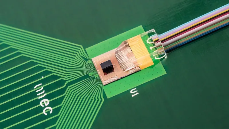
Nvidia's reasoning for pouring $4 billion into silicon photonics is simple: the physical limits of copper wiring have finally arrived. No matter how high you stack HBM, no matter how fine the process node, a moment comes when the copper interconnects linking one chip to another become the bottleneck.
The Thermal Hell Copper Built, and the Exit Light Opens
The more advanced AI computation becomes, the more a data center turns into a giant furnace. Copper wires carrying electric current inevitably heat up because of resistance, and that heat forces chips into throttling that caps their performance. It is exactly why Big Tech is pouring trillions of won into liquid cooling.
Light is different. With almost no resistance, it produces almost no heat. The moment you pull out the copper and plant light in its place, a data center's energy efficiency soars and cooling costs drop by more than 70 percent. That is precisely why Nvidia and TSMC are fixated on this "alliance of light."
From Stacking to Connecting: The Battlefield Has Moved
Until now, Korea's Samsung and SK hynix have concentrated on stacking HBM higher and denser. Samsung has declared it will advance its logic die to two nanometers starting with HBM4E, while SK hynix has countered by holding to a more cost-efficient 12-nanometer process and competing on packaging technology instead.
But in the silicon photonics era, "how well you connect with light" matters more than "how high you stack." However superior your stacking technology, falling behind in the optical interconnect that links chip to memory through light carries a real risk: being reduced to a simple parts supplier.
The Post-HBM Blueprint Silicon Valley Is Drawing
Google and Microsoft have already begun grafting silicon photonics into their own dedicated data centers. They are no longer bound by the grammar of the copper era. Through light, they are constructing a "neural network of light" that ties an entire sprawling data center into a single, organic supercomputer.
For Korea's HBM to play a central role in this grand blueprint — rather than serving as a simple consumable — it has to shift its technological paradigm. There is no time to stay buried in the memory-stacking race.
Beyond Manufacturing Supremacy, Sovereignty Over Transmission
In the end, semiconductor supremacy is moving past the manufacturing stage and into the "transmission stage." The contest over who can make it smaller and who can stack it higher is being recast as a contest over who can send it faster and more efficiently.
Silicon photonics is not merely a transmission technology. By moving data at the speed of light while maximizing energy efficiency, it is set to become the core infrastructure that decides the future balance of AI power. Will Korea join as a leading architect of this neural network of light that Silicon Valley has designed — or remain a mere supplier? The future of the country's semiconductor industry hangs on the answer.
As the copper era fades and an empire of light rises, Korea's semiconductor industry stands at an unprecedented crossroads. If it cannot move beyond the world's best stacking technology to secure the world's best "light-connection technology," the memory-superpower standing it has defended for the past three decades is bound to face a new kind of challenge.